ジュエリーの金メッキの検査と修復方法
Gold Plating Testing & Recovery: Thickness, Hardness, Stress, Wear & Eco-Friendly Recycling for Jewelry
はじめに
Wondering how to ensure the quality of gold plating on your jewelry? This article dives into various testing methods for gold plating thickness, hardness, internal stress, and wear resistance. Learn what techniques like microscope measurement, chemical dissolution, and fluorescent X-ray can do. Plus, discover why gold recovery from waste is crucial and how to do it. Essential reading for jewelry stores, studios, brands, and designers aiming for top-notch quality and sustainability.

宝飾品の金メッキの検査と修復方法
目次
Section I Physical Property Testing of the Gold Plating Layer
1. Thickness
Table 1-137 Overview of Gold Plating Layer Thickness Measurement Methods
| そうだ。 | Measurement Method | モデル | Measuring range/μm | Precision | Time required/min | Proficiency required | Commercially available equipment | 備考 |
|---|---|---|---|---|---|---|---|---|
| 1 | Microscope method (section) | P,D | Above 2 |
2%(5μm) 10%(2μm) 50%(lμm)
|
60〜90 | 高い | Available | Suitable for measuring the thickness of 2μm or more over a wide range, and for measuring the inner surface. |
| 2 | Chord Method | P,D | Above 2 | Same as 1 | 5 | ミディアム | Available | Applicable at work site |
| 3 | Interference Microscopy | P,N(D) | 0〜20 | 0. 5% | 5 | 高い | Available | Reliability measurement of very thin layers |
| 4 | Chemical Dissolution Method | S,D | Above 0 | 0.5% 〜 1% | 20 | 高い | - | Applicable to pure gold plating and gold foil remaining after dissolution of the substrate. |
| 5 | Gravimetric method | S | Above 0 | 0. 5%〜 1% | 3〜5 | 高い | - | Control of average thickness of plated layer |
| 6 | Anodic Dissolution | S,D | 0. 5〜 0. 7 | Same as 1 | 3〜5 | ミディアム | Available | Measurement of fine wires |
| 7 | Fluorescence X-ray | S,N | 0〜5 | 0. 5% | 3〜5 | ミディアム | Available | Suitable for quality control |
| 8 | Beta-ray backscattering | S,N | 0. 25〜 2. 5 | 1% 〜2% | 2〜3 | ミディアム | Available | Suitable for quality control |
| 9 | Electron probe method | S,N | Above 0 | - | - | 高い | Available | - |
| 10 | Profilome-try | P,N(D) | 0〜10 | Same as 3 | 3〜5 | ミディアム | Available | - |
The following introduces commonly used daily methods.
(1) Microscope Method
① Sample preparation method: The embedding, grinding, etc., of the sample must be performed by highly skilled technicians. Low-temperature operation is required to prevent thermal diffusion between the material and the gold plating layer when embedding the sample in resin.
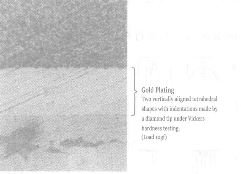
From coarse grinding to the final fine grinding with diamond abrasive below 1μm, excessive grinding time must be avoided to ensure the smoothness of the grinding surface. This is especially important when there is a significant hardness difference between the plating layer, the substrate material, or the protective layer. In particular, collapse easily occurs between multiple metal layers, causing measurement errors of the boundary line (Figure 1-114).
② Causes of errors in microscopic measurement of cross-sections
- a. Errors caused by improper embedding, especially the high likelihood of errors in inclined cross-sections.
- b. During grinding, over-etching must be performed if the coating cracks or collapses, which easily leads to errors. Errors caused by this reason are particularly likely to occur in inclined cross-sections. Moreover, the boundary line will be unclear if the grinding debris from rough grinding is not thoroughly removed.
- c. Errors caused by insufficient microscope magnification (when 1~2μm, measurement is done at 1000x).
- d. Errors caused by instrument equipment due to lens shaking, operation, etc.
- When measuring coating thickness with a microscope, errors may occur due to sample setup and operator proficiency. However, the coating thickness of 2μm is generally measured within the measurement limit, at which point the accuracy is about ±10%.
③ The advantages and disadvantages of the microscope method are shown in Table 1-138.
Table 1-138 Comparison of the Advantages and Disadvantages of the Microscope Method
| メリット | デメリット |
|---|---|
|
① It is independent of the thickness of the plated layer and can be measured directly. ② Thickness distribution of the plating along the cut surface and the whole plating can be measured. ③ The combination of plating layer and base layer can be measured, and each layer can be measured separately. ④ Measurement is possible on all sides regardless of the shape of the sample. ⑤ The structure and quality characteristics of bonded crystals can be generally examined from the cross-section, and the hardness of the sample can be measured. ⑥ One of the most accurate measurement methods for thicknesses of 2.5um or more.
|
① Destructive test ② Time-consuming (60~90min depending on the hardening time of the resin) ③ Measurer's experience is very important, but it is not easy to be accurate for thin plating.
|
(2) Chemical Dissolution Method
Cut a portion of the sample and dissolve it into foil form using nitric acid. After thoroughly washing with water, clean again with alcohol or acetone, dry, and weigh (however, this method may cause errors for coatings other than pure gold). The calculation of coating thickness is as follows:

式の中で、
W— the quality of the coating, g;
a— the area of the coating, cm2;
d— the density of the coating, g/cm2.
If the coating area is sufficient, this detection method has high accuracy. Since the mass of 1cm2, 1μm gold is 0.00193 g, and the balance measurement accuracy is 0.00002 g, the measurement accuracy is 1%. Therefore, increasing the measurement area can also ensure accuracy when the gold plating layer is very thin. The advantages and disadvantages of this measurement method are shown in Table 1-139.
Table 1-139 Advantages and Disadvantages of Chemical Dissolution Method for Thickness Measurement
| メリット | デメリット |
|---|---|
|
High accuracy over a wide range of coating thicknesses Measurement is independent of the size and shape of the sample
|
It is difficult to measure the area of curved surfaces and complex shapes. Indirect method for destructive measurements Daily measurements are performed irregularly Requires a high level of skill Not applicable to gold plating on substrates that do not dissolve in nitric acid, such as Zn-Pb alloys and stainless steel.
|
(3) Gold Plating Layer Peeling Method
When the material is insoluble in nitric acid, gold can be selectively dissolved and then measured. Gold is dissolved electrolytically in a sodium cyanide–sodium hydroxide solution, and the plating thickness is calculated from the weight of the gold.
(4) Gravimetric Method Before and After Gold Plating
Calculate the thickness of the plating layer using the weight increase from electroplating.
In those above (2) ~ (4), when plating a gold alloy layer, the thickness of the plating layer can be calculated with high precision by using atomic absorption spectroscopy to measure the co-deposited metals other than gold.
(5) Anodic Electrolytic Method
First, small indentations are pressed on the sample, and the coating to be measured is dissolved at the indentations by a certain anodic current. The anodic efficiency in the indentations serves as 100%, and the endpoint is reached when the voltage changes as the base metal is exposed. The thickness of the coating is proportional to the dissolution time.
Different compositions can be selected according to the metal being measured. For example, when measuring gold on silver, copper, and nickel, magnesium chloride (200g/L) and sodium chloride (100g/L) solutions are used.
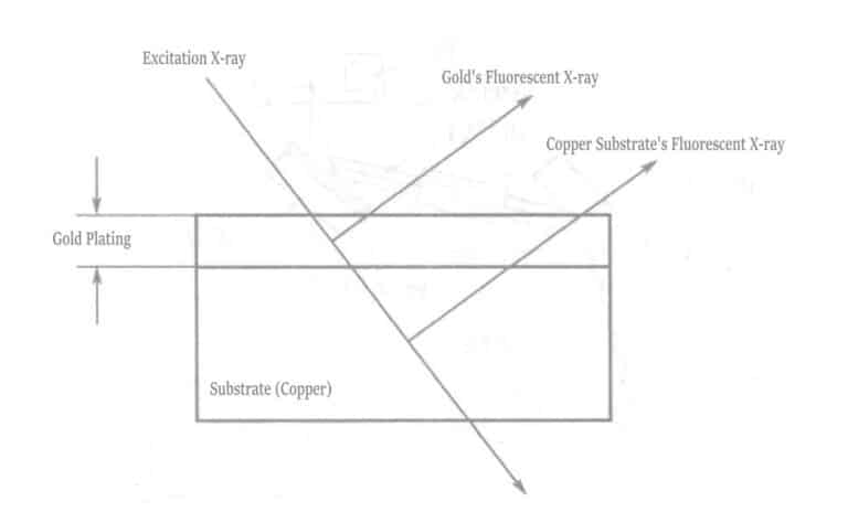
(6) Fluorescent Ray Thickness Measurement
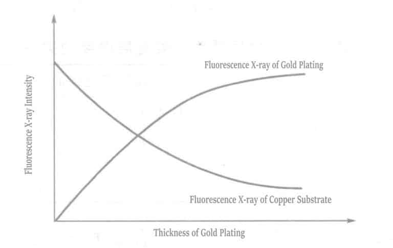
When X-rays or other radiation collide with matter, the characteristic X-rays of the elements inherent in the matter are excited. These X-rays are called characteristic X-rays or fluorescent X-rays. To generate fluorescent X-rays, the elements constituting the matter must be excited, and the radiation that excites the fluorescent X-rays when colliding with the matter is called exciting radiation. Figure 1-115 shows that when a sample composed of a substrate material and a plating layer is irradiated with exciting X-rays, different fluorescent X-rays are excited from the substrate and the plating layer. The relationship between plating thickness and fluorescent X-ray intensity is shown in Figure 1-116. As the plating thickness increases, the fluorescent X-ray intensity of the plating layer increases. In contrast, the fluorescent X-ray intensity of the substrate material decreases due to absorption by the plating layer.
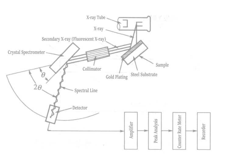
The measurement range of the gold plating thickness is approximately 0.05~8.0μm (within an accuracy of 0.5%). The materials that can be measured with the gold plating layer include copper or copper alloys, iron, cobalt, nickel, aluminum, stainless steel, 42 alloy, ceramics, etc. Measurement is relatively difficult when the material is silver, molybdenum, bismuth, etc., with a nickel-plating base layer and a gold-plating surface layer. The reason is that the X-rays of gold are affected by the X-rays of silver and molybdenum materials, causing changes in intensity, and it is difficult to distinguish between the X-rays of tungsten and gold.
When the material contains electroplated layer components and the atomic numbers of the electroplated layer and the material differ by within 3, measurement is difficult, and the accuracy of the measurement is also low.
For double-sided electroplated layers, when the substrate material is , the fluorescence X-rays from the electroplated layer on the reverse side penetrate the material, causing the measured value to be greater than the actual thickness of the electroplated layer. The relationship between the thickness of the substrate material and the electroplated layer thickness is shown in Table 1-140.
Table 1-140 Relationship between Material Thickness and Gold Plating Thickness
| Material Thickness/mm | Rate Increasing with Thickness/% | |
|---|---|---|
| Material:Cu | Material:Fe | |
| 0. 03 | 1.37 | 4.1 |
| 0. 04 | 0.33 | 1.4 |
| 0. 05 | - | 0.5 |
When the gold plating layer is especially a non-pure gold plating layer, measurement errors may occur due to the alloy ratio, so it is necessary to first produce standard samples and detection lines.
B.J. Cross and others have detailed the accuracy of fluorescence X-ray measurement of plating thickness.
2.硬度
The hardness of the gold plating layer is related to the structure of the plating, the co-deposited impurities, or both. The hardness of acidic gold plating layers has a linear relationship with the added metal concentration. By changing the concentration of ligands in the plating solution, the hardness of the plating layer can be adjusted.
The brightness and hardness of bright gold plating layers using organic brighteners increase proportionally with the concentration of brighteners in the plating solution. This is due to the increased amount of co-deposited substances in the plating layer and the promotion of particle refinement. However, the current situation, as shown in Table 1-141, indicates that the relationship between hardness and wear resistance is not linear.
Table 1-141 Relationship between Hardness and Wear Resistance of Gold Alloy Plating Layers
| Eutectic metal content/% | Types of plating solution | Hardness (load 25gf) /(kgf/mm2) | 耐摩耗性① /[mg/(h • cm2)] |
|---|---|---|---|
| なし | Acidity(65℃) | 52 〜 129 | 0.07 |
| なし | Potassium cyanide(65C) | 47 〜 86 | 0.15 |
| なし | Neutral(65℃) | 44 〜 82 | 0.50 |
| Cd 1.4% | Alkaline-Cyanide(50℃) | 176 〜 236 | 0.15 |
| Co 0. 1 % | Acidity(35℃) | 137 〜 196 | 0.68 |
| Co 0. 9% | Acidity(35℃) | 194 〜 238 | 0.70 |
| Ni 0. 1% | Acidity(35℃) | 135 〜 167 | 1.01 |
| Ni 1. 0% | Acidity(35℃) | 167 〜 206 | 0.23 |
| Ni 18% | Acidity(35℃) | 194 〜 238 | 0.51 |
Wilson and Cullent provided detailed explanations regarding the hardness of the gold plating layer. When measuring the hardness of the gold plating layer, the following three key issues must be noted.
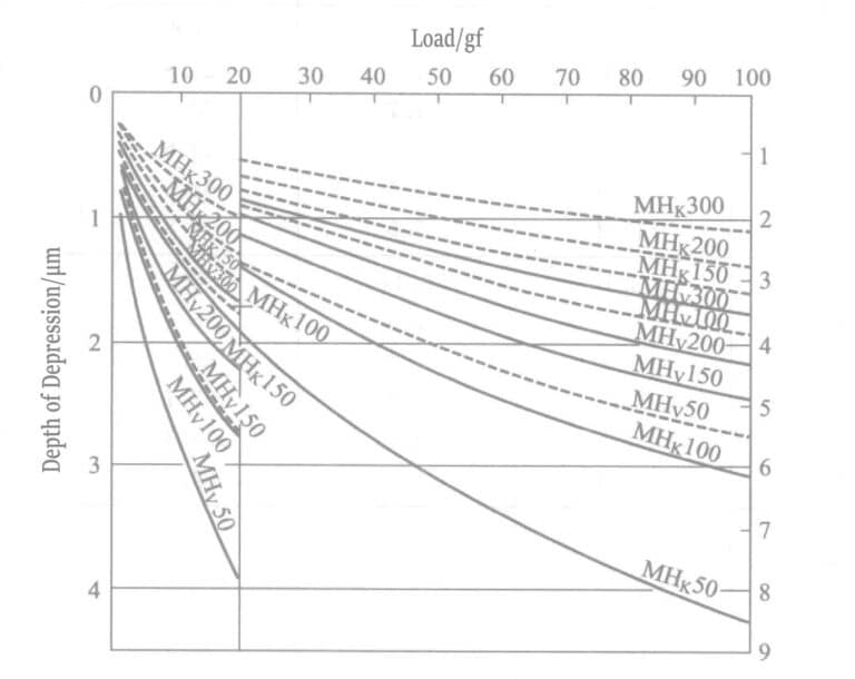
(1) Thickness of the gold plating layer
Usually, the actual usable thickness of the gold plating layer is only a thin layer around 1μm, and due to the severe influence of the underlying plating layer, the surface hardness cannot be directly measured. Table 1-142 shows the minimum required thickness for measuring the surface hardness of the gold plating layer. The general hardness of the gold plating layer is Hv 200 to 300, and the required thickness for measurement is about 20μm. HK corresponds to 10~15μm.
Table 1-142 Minimum Required Thickness for Measuring the Surface Hardness of Gold Plating (Load 25 gf) Unit: μm
| 硬度 | Vickers Hardness | Nup Hardness | 硬度 | Vickers Hardness | Nup Hardness |
|---|---|---|---|---|---|
| 50 | 43 | 30 | 200 | 21 | 14 |
| 100 | 30 | 20 | 300 | 18 | 11 |
| 150 | 24 | 16 |
(2) Indentation Type
Two main types of indenters are used: the Vickers method and the Nup method, which uses a diamond pyramid-shaped indenter. The characteristics of the two indenters are shown in Table 1-143.
There is a significant difference between the Vickers and Nup hardness testing methods, reflected in the diagonal length and indentation depth on the surface of the electroplated layer.
Table 1-143 Characteristics of Diamond Indentations in Vickers Hardness and Nup Hardness Tests
| 項目 | Vickers | Nup |
|---|---|---|
| Condition of indentation |
|
|
| Shape and size of indentation under the same load |
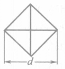
|
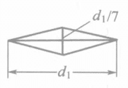
|
| Depth of indentation | d/7 | d1/30 |
| Minor hardness/(kg/cm2) |

|
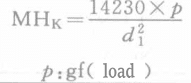
|
(3) Selection of Load
① Surface Measurement: To avoid the influence of the substrate material, the thickness of the electroplated layer for hardness testing must generally be 10 times the indentation depth. When the hardness of the electroplated layer is approximately the same as that of the substrate material, a thickness of 3~5 times is also acceptable. Table 1-144 shows the relationship between load variation within a certain hardness range and the indentation depth of Vickers and Nup hardness tests.
Table 1-144 Diagonal Length and Indentation Depth
| 硬度 | 荷重/gf | Vickers | Nup | ||
|---|---|---|---|---|---|
| Diagonal length/μm | Indentation depth/μm | Diagonal length/μm | Indentation depth/μm | ||
| 50 |
1 5 10 20 50 100 |
6. 1 13. 6 19. 3 27. 2 43. 1 60. 9 |
0. 9 1. 9 2.8 3. 9 6. 2 8. 7 |
16. 9 37. 7 53. 4 84. 6 119. 3 168. 7 |
0. 6 1.3 1. 8 2. 8 4. 0 5. 6 |
| 100 |
1 5 10 20 50 100 |
4. 3 9. 6 13. 6 19. 3 30. 5 43. 1 |
0. 6 1. 4 1. 9 2. 8 4. 4 6. 2 |
11. 9 26. 7 37. 7 53. 4 84.4 119. 3
|
0. 4 0. 9 1. 3 1. 8 2.8 4.0 |
| 150 |
1 5 10 20 50 100 |
3. 5 7. 9 11. 1 15. 7 24. 3 35. 2 |
0. 5 1. 5 1. 7 2. 2 3. 5 5.0 |
9. 8 21. 8 30. 8 43. 6 68. 9 97. 5 |
0. 3 0. 6 0. 9 1. 3 2. 0 2. 8 |
| 200 |
1 5 10 20 50 100 |
3. 1 6. 8 9. 6 13. 6 21. 5 30. 5 |
0. 44 1.0 1. 4 1. 9 3. 1 4. 4 |
8.4 18.9 26. 7 37. 7 59. 7 84. 4 |
0. 3 0. 6 0. 9 1. 3 2. 0 2. 8 |
| 300 |
1 5 10 20 50 100 |
2. 5 5. 6 7. 9 11. 1 17. 6 24. 9 |
0. 35 0. 5 1. 1 1. 7 2. 5 3. 6 |
6. 9 15. 4 21.8 30. 8 48. 7 68. 9 |
0. 2 0. 5 0. 7 1. 0 1. 6 2. 3 |
Table 1-145 Changes in Hardness with Varying Loads on Gold Plating Layers and Gold Blocks
| Gold plating layer | Load /gf | 2 | 4 | 5 | 10 | 25 | 50 | 100 |
| Hv | 61.1 | 70 | 76 | 82 | 106 | 102 | 105 | |
| Gold block | Load /gf | 1 | 5 | 10 | 25 | 50 | 100 | |
| Hv | 29 | 40 | 54 | 65 | 68 | 72 |
② Cross-sectional measurement
Cross-sectional measurement is less affected by material properties, but the measurement is very difficult. The minimum required thickness for measuring the cross-sectional hardness of the gold plating layer is shown in Table 1-146, and the cross-sectional measurement photo is shown in Figure 1-119.
Table 1-146 Minimum Required Thickness for Measuring Cross-Sectional Hardness (25 gf)
| 硬度 | Minimum thickness/μm | 硬度 | Minimum thickness/μm | ||
|---|---|---|---|---|---|
| Vickers | Nup | Vickers | Nup | ||
| 50 | 69 | 26 | 200 | 26 | 12 |
| 100 | 42 | 18 | 300 | 25 | 10 |
| 150 | 33 | 14 | |||
3. Internal Stress
3.1 Principle of Internal Stress
Almost all electroplated layers have internal stress. Internal stress causes cracks, bubbles and peeling in the electroplated layer, and it has also been denied as direct causes. Therefore, the cause of internal stress has not yet been definitively concluded. The following two theories can reference the gold plating layer.
(1) Excess energy: Metal ions must overcome an energy barrier to detach from ligands and enter metal crystallization; this energy barrier is the cause of polarization. When surpassing the energy barrier, the excess energy possessed by the atoms is converted into heat. Hence, the newly precipitated plating layer is hotter than other metals, generating tensile stress during cooling.
This theory explains the high-stress value of acidic gold plating and the low-stress value of sulfite gold plating.
(2) Transfer theory: Impurities entering the metal crystallization form crystal defects that cause stress in acidic gold and sulfite gold. Empirically, it is determined that high stress exists in electroplated layers containing more than 0.3% cobalt or nickel, a phenomenon consistent with the transfer theory. Many factors cause stress, and a single theory cannot comprehensively explain it.
The generally recognized internal stress refers to the stress that can be measured using a spiral pressure gauge and IS measuring instrument; this type of stress is called “macroscopic stress.” Stress that can only be measured by X-ray diffraction and electron beam diffraction is called “microscopic stress”.
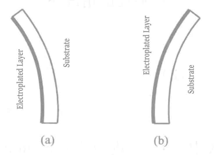
When plating on one side of an extremely thin metal material, if there is internal stress (macroscopic stress) in the plating layer, bending will occur as shown in Figure 1-120. The bending in Figure (a) results from tensile stress, while Figure (b) results from compressive stress.
3.2 Determination of Internal Stress
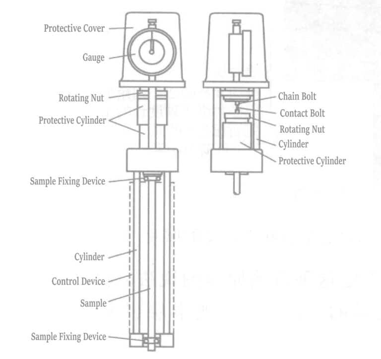
There are many methods for determining the macroscopic stress of electroplated layers. Commonly used instruments include the Brenner-Senderoff type stress meter (spiral pressure gauge) and the IS measuring instrument.
The construction of the IS measuring instrument is shown in Figure 1-121.
According to Dvorak’s method, plating is performed on both sides of a flat, thin plate or wire-like specimen. During the electrodeposition process, the elongation or contraction of a specimen of known length is accurately detected. Using the known elastic modulus of the plane and the measured elongation and contraction values when a plating layer of a certain thickness is deposited, the average internal tensile or compressive stress acting on the entire cross-section of the electroplated layer is calculated using formulas (1-32) and (1-33).
(1) In the case of a flat plate

式の中で、
σ — internal stress, N/mm2;
E— elastic coefficient of the flat plate or iron wire, N/mm2;
d—— Thickness of the plate, mm;
x—— Change in length, mm;
l—— Length of the plate, mm;
t—— Thickness of the plating layer, mm.
The internal stress and friction wear characteristics of the gold plating layer measured by the IS tester are shown in Table 1-147.
Table 1-147 Hardness, Internal Stress, and Friction Wear Characteristics of Gold and Gold Alloy Coatings
| 電気めっき液 | Composition of the coating/% | 硬度 Hv20 | Hardness Friction and wear | Internal stress (5μm)/(N/mm2) |
|---|---|---|---|---|
| オー | 99. 99 | 60〜70 | 1 | 13. 7〜27. 5 |
| Au-Co | 99. 8-0. 2 | 120〜180 | 10 | 137 |
| Au-Ni | 99. 6-0. 4 | 140〜170 | 10 | 132 |
| オー | 99.9 | 100〜180 | 2 | 13. 7〜27. 5 |
| Au-Cu | 99-1 | 160〜240 | 4 | 34. 3〜68. 7 |
| Au-Cu | 67-33 | 380〜400 | 7 | 15.7 |
|
注釈 1. Gold, gold-cobalt, gold-nickel: weakly acidic potassium gold chloride plating solution; gold, gold-copper, gold-copper: neutral sulfite plating solution. 2. 1—high wear amount; 10—low wear amount.
|
||||
Due to appropriate alloying or the co-deposition of organic additives, the wear resistance of the gold plating layer is significantly improved, and this type of gold plating layer is characterized by high internal stress.
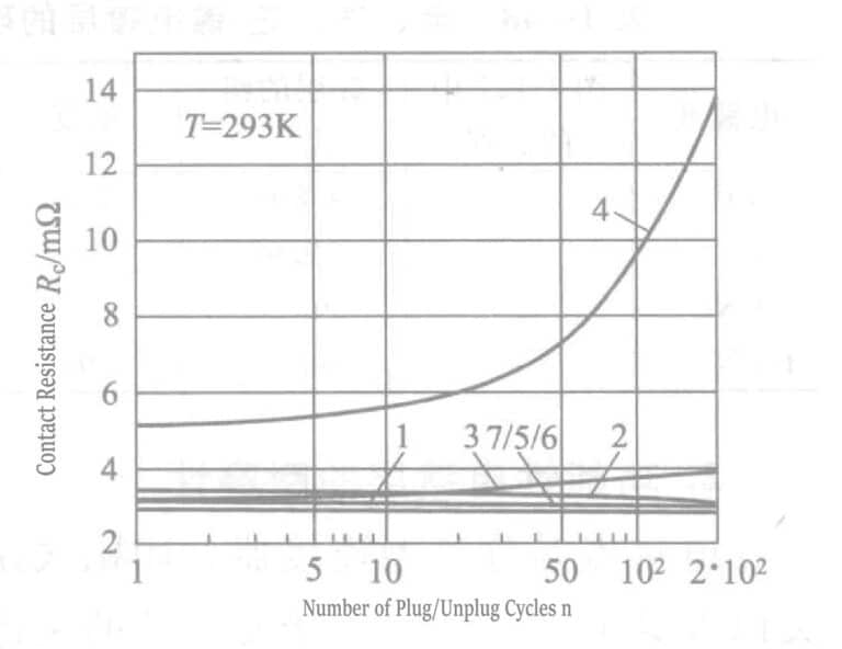
Measurement was conducted on palladium and palladium-nickel alloy coatings as alternatives to gold plating, and characteristic values of internal stress were obtained. After plugging and unplugging the connector’s plug and socket 200 times, the contact resistance RC was measured to compare wear resistance. If the nickel content in the coating is increased, a mixed crystallization of palladium and nickel occurs in the palladium-nickel alloy coating. With the increase of nickel content in the coating, the contact resistance after 200 plug-unplug cycles significantly increase in contact resistance and decrease in tensile stress.
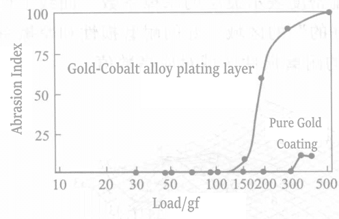
In the plating layers in Figure 1-122, curves 1 to 7, the brush plating of the wear-reducing material gold-cobalt alloy layer (curves 5 to 7) shows the same excellent characteristics as the cobalt alloyed, hardened gold-plated layer with organic matter because of the high hardness and significant reduction of loss.
4. Wear Resistance
4.1 Wear Resistance of Decorative Plating Layers
Because gold plating layers are usually thin due to the high price of gold, plating layers on products frequently touched by hand require sample production and a trial period before being officially plated after passing the evaluation. This method often takes a lot of time and may not yield reliable results. Accelerated testing is a method that can quickly compare the wear resistance of plating layers within a short time.
The method by R. Duva and F. I. Nobl: A certain amount of sand is dropped from a certain height onto the plating surface, and then the amount of gold worn away is calculated. Alternatively, the plated part is rotated in the sand to compare the reduction of gold after sand friction. Wear resistance testing method for portable items: rubbing the plated part on canvas or cowhide. This wear resistance test method is relatively practical. The amount of wear is calculated by measuring the thickness with a film thickness gauge. Table 1-148 shows the hardness, contact resistance, and internal stress values of gold and gold alloy plating layers.
Table 1-148 Hardness, Contact Resistance, and Internal Stress of Gold, Palladium, and Palladium-Nickle Alloy Plating Layers
| Plating solution | Data in Figure 1-122 | The composition of the Plating Layer /% | 硬度 | Contact resistance after 200 insertions and removals/mΩ | Internal stress (4/μm)/(N/mm2) |
|---|---|---|---|---|---|
| Au-Co | 1 | 99. 8-0. 2 | 180 | 2. 9〜2. 9 | 120 |
| 博士号 | 2 | 99. 99 | 318 | 3. 4〜3.0 | 220 |
| Pd-Ni | 3 | 80-20 | 316 | 3〜4 | 115 |
| Pd-Ni | 4 | 65-35 | 500 | 5〜14 | 60 |
4.2 Wear Resistance of Functional Plating Layer
Electrical contacts are separable connectors and are key components in printed circuit boards, mechanical sliding plates of equipment, switches, and other electronic components for current transmission. The contact resistance of the contact surfaces must be low, so gold and other precious metals are widely used. Gold does not react with the atmosphere or form an oxide film, whereas other precious metals, such as palladium, platinum, and rhodium, have some oxide films. Although these oxide films can be removed by mechanical, chemical, electrochemical, or heating methods, the design must consider the normal electrical connection of the product during its service life.
The plating layer on the contact point is generally thin, and during sliding operations, it is necessary to avoid the exposure of the base material and the underlying plating layeras much as possible, as well as maintaining the integrity of the plating layer, make comprehensive lubrication technology very important.
The number of contact points in separable connectors continuously increases, making low wear increasingly important. When designing surface treatment schemes, corrosion resistance, discoloration resistance, and contact resistance thermal stability are all important quality indicators. For example, adding cobalt or nickel to the gold plating solution, using palladium-nickel alloy to replace gold, brushing gold plating on palladium-nickel alloy, and using a nickel-based plating layer are all effective methods to improve the tribological performance of contact plating layers. Table 1-149 classifies materials used for electrical contacts based on performance.
Table 1-149 Classification of Materials Used for Electrical Contacts
| 分類 | Properties of connectors | Contact metal |
|---|---|---|
| Grade A (best) | Metals that essentially do not generate a surface film, with low contact stresses metal to metal direct contact | Gold and high percentage gold alloys |
| Grade B | Metals with little or no surface film generation, requiring higher contact stresses than gold (especially in the long term) | Platinum group metals, platinum, palladium, iridium, rhenium, etc. |
| Grade C | Metals that generate surface films under certain conditions, requiring sliding and higher contact stresses | Nickel, silver and high percentage gold alloys |
| Grade D | Non-precious metal series metals, generate thick and strong film of the metal, the need for high contact stress, through the film conductivity | Copper, nickel, tungsten, copper alloys, aluminum, tin |
コピーライト @ Sobling.Jewelry - ジュエリー カスタムジュエリーメーカー、OEMおよびODMジュエリー工場
4.3 Contact Wear
4.4 Contact Gold Plating
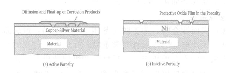
The porosity of the gold plating layer surface is highly detrimental. Corrosion reaction products accumulate in the pores of the plating layer and diffuse upward along the pore walls. When reaching the contact surface, they insulate the contact, increasing the contact resistance of the plating layer. When the substrate metal is inactive, the harmful effects of porosity are significantly reduced for corrosion-resistant metals (such as palladium) or metals that form non-diffusive films (nickel).
One function of the nickel base layer in precious metal plating is to form a thin oxide film at the pores of the precious metal plating layer, and nickel itself can also block the diffusion of corrosion products. Exposed base metal edges become corrosion sources, but if a nickel base plating layer exists, it can inhibit the spread of corrosion. The corrosion diffusion rate in the nickel plating layer is very slow, but once corrosion products reach the precious metal plating layer, they diffuse quickly. Nickel also has another diffusion-preventing function, preventing zinc or copper from brass or copper substrates from diffusing and contaminating the gold plating layer. The diffusion rate of copper in nickel is two orders of magnitude lower than that in gold, palladium, or silver. Additionally, nickel serves as a hard support layer as a base plating layer, improving the lifespan of the gold plating layer. Consequently, the wear life of the gold plating layer is significantly enhanced. Figure 1-124 is a schematic diagram of the above corrosion process.
4.5 Adhesive Wear
The wear mechanism of the gold plating layer is adhesive wear. M. Antler studied the properties affecting wear behavior. Table 1-139 shows the mechanical properties of gold plating layers obtained by the DC method, listing the durability of various gold and gold alloys from low to high. The cobalt-hardened gold plating layer has the best wear resistance, followed by gold-silver and gold-cadmium alloys.
There are various speculations about the reasons for poor wear behavior. Compared with soft pure gold, cobalt and nickel hard gold plating layers have better resistance to adhesive wear, which is considered to be due to hardness. However, compared with forged gold alloys of the same hardness, hard gold plating layers perform worse, indicating that the hardness explanation is not entirely correct.
Therefore, the poor wear resistance of hard, relatively pure gold plating layers (24K hard gold in Table 1-150) cannot be explained by hardness. Later, it was proposed that organic polymers in cobalt and nickel hard gold plating layers may act as lubricants.
Table 1-150 Properties of Various Gold Plating Layers in DC Electroplating
| シリアル番号 | Types of Gold | Types of Electroplating Solutions | Alloy metal | C/% | Hardness /(kgf/mm2) | Extension /% |
|---|---|---|---|---|---|---|
| 1 | Soft, High Purity, Acidic, No Brightness | Cyanide, Citrate Buffered | なし | 0.01 | 50 | >10 |
| 2 | 24K, hard gold | Cyanide | なし | 0.01 | 200 | >10 |
| 3 | AFHG① | Cyanide | なし | 0.06 | 180 | 2.5 |
| 4 | Alloy Electroplate, Alkaline, Cyanide Free, Bright | Sulfite | 0. 7% Cd | なし | 135 | 5 ~10 |
| 5 | Alloy Electroplate, Alkaline, Cyanide Free, Bright | Cyanide | 1% Ag | 0.07 | 140 | 0.75 |
| 6 | Acid, Hard, Bright | Cyanide | 0. 15% Co | 0.15 | 180 | <0. 4 |
Table 1-150’s analysis results of medium carbon indicates the polymer content in the electroplated layer. However, hard gold electroplated layers containing certain organic polymers experience adhesive wear more severely than cobalt or nickel hard gold plating layers, which also shows that the explanation based on hardness is inappropriate. Alkaline silver cyanide plating solution and AFHG (additive-free hard gold, a pure gold hard plating solution advocated by Dr. Okinaka) are similar examples. Moreover, even cobalt-hardened gold plating layers containing a large amount of polymer can cause wear due to the formation of protrusions under low load when the surface is not clean.
(1) A long-term lack of correct understanding of wear on gold plating layers.
① Insufficient knowledge about the structure of eutectic polymers.
② Insufficient understanding of the physical properties of gold plating layers beyond hardness. Table 1-139 also includes the ductility of gold plating layers.
The structure of the cobalt-hardened gold plating layer indicates that some polymers are formed by cobalt ligands, with 2~7nm particles uniformly distributed in the plating layer, including some larger particles. From the metallurgical theoretical analysis of the effect of dispersed particles on the solid mechanical properties, the eutectic phase is the cause of hardness and low ductility. The most durable plating layers have relatively low ductility (such as an elongation 0.4%). Except for the drill-hardened gold plating layer in Table 1-139 (No. 6 plating solution), the hard gold plating layers containing polymers, 0.28% nickel-gold plating layers, 1.3% cobalt, and 0.55% indium have the same wear resistance and mechanical properties.
(2) Affecting contact adhesion wear, the key to achieving the best performance
① Reduce the initial contact area and increase hardness.
② Reduce the low ductility caused by bone growth.
③ Lubrication to suppress adhesion at contact points.
Thus, regardless of the presence or absence of eutectic polymers, hardness alone does not achieve good wear resistance. Accompanied by low-ductility hardness, better performance can be demonstrated. At the same time, if the gold plating layer is too brittle, it will also be damaged under normal loads.
Contact lubricants can compensate for the poor wear resistance of ductile gold plating layers. Changing the plating current’s waveform can alter the gold plating layer’s composition, structure, and properties. For example, compared to the DC plating layer using the same plating solution, the cyanide-hardened gold plating layer contains almost no polymers. Both pulse and DC plating have the same cobalt content and hardness in the gold plating layer. However, according to bending test results, the DC cobalt-hardened gold plating layer shows very low ductility, and sliding test results indicate that it is difficult to produce adhesive wear. These facts are consistent with the analysis that ductility is unfavorable for wear resistance.
4.6 Wear of High-Speed Gold Plating
In high-speed gold plating solutions, the plating solution composition and conditions were changed for plating, and a friction test device constructed with sliders/flat plates was used to test the performance of connector contacts. The contact surfaces were all plated with 5μm gold, and a sliding test was conducted for 500 cycles under a 150 gf load.
Figure 1-125 shows partial results of the wear test. The corresponding cobalt content in the plating layer, the cobalt concentration in the plating solution and the plating current density indicate the friction coefficient of the plating layer. The marked areas on the curve represent regions with “good” wear resistance. Good wear resistance corresponds to friction coefficient values below 0.26, while poor wear resistance regions correspond to higher values.

Figure 1-125 Effect of cobalt concentration and current density in the plating solution on the K value of the plating layer
(+ indicates "excellent" or "very good" wear characteristics; values on the curve are friction coefficients)
4.7 Cutting Wear
Cutting wear occurs when the contacting material is rough and relatively hard, causing the surface to be gouged. The material being cut separates in the form of chips and moves along the sides of the groove without forming free particles. Compared to compressive strength, materials with low tensile strength are prone to brittle failure, producing cracks along the wear track during sliding. Many contact materials, such as rhodium and gold-cobalt, are relatively brittle and are easily damaged during cutting.
For example, compared to forged precious metal contact materials with cladding and the same materials after electroplating, the former has ductility and excellent resistance to cutting wear. The two-body wear coefficient of pure gold cladding and gold-cobalt alloy electroplated layers of the same thickness was measured using a diamond stylus to scratch the surface of the plated layer.
The determination of wear is performed using the electrochemical method. The chemically treated wet paper is placed on the worn specimen, and a direct current voltage is applied. Wear marks appear on the paper, with the colored parts indicating the exposed material. The wear value is 100 times the ratio of the length of the colored marks to the total length of the marks.
As shown in Figure 1-126, although the gold-cobalt alloy plating layer is supported by the hard base plating layer and substrate, the wear resistance of the overlay metal is better. Similarly, the adhesive wear of pure gold is worse than that of the gold-cobalt alloy plating layer. In the extensive use of precious metal contacts, adhesive wear is more important than brittle fracture wear caused by cutting. The initial adhesive wear characteristics should be considered when selecting electrical contact materials. When using lubricants that can mitigate adhesive wear, metals with good cutting wear performance should be used as much as possible.
4.8 Fretting Wear
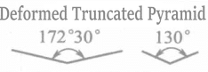
Fretting wear occurs generally at very small amplitude vibrations below 130μm.
(1) Causes of vibration
①The shaking of the printed circuit board of the edge connector;
② Vibrations transmitted to the contact point through the wires;
③ Electromagnetic-induced vibrations or thermal deformation between materials with different thermal expansion coefficients.
Friction has long been overlooked in gold-plated contacts and was only recognized after using cheap substitutes easily damaged by friction. Low-performance contacts such as tin or tin-lead alloys have had friction and have been considered a problem for a long time.
Tin is always covered with an oxide film. Therefore, tin-plated connectors must remove the oxide film to maintain metal-to-metal contact. Fortunately, the oxide film on the tin is thin, hard, and brittle and can be easily broken by vertical stress on the surface, making it very easy to remove.
The tin beneath the oxide film is soft and easily deformed. As the tin flows, the cracks in the oxide film expand. The tin exposed through the cracks becomes the contact surface. Therefore, under low load, the contact resistance value of the tin contact point is the same as that of gold under the same load. However, once an intermetallic contact is formed, the interface does not hinder the contact area, and it is very stable. If the interface is obstructed, the tin exposed to the atmosphere will oxidize again. This is a phenomenon of interface disorder. Small periodic vibrations (friction) mainly cause tin contact degradation.
Very short periodic micro-vibrations destroy the contact points of the tin interface, exposing parts of the tin to oxidation resulting in the generation of Sn/Sn oxide film debris, which increases the contact resistance. This frictional movement and oxidation together are called wear. Laboratory studies on contact materials’ friction and wear phenomena are also very common. M. Antler conducted experiments using the apparatus shown in Figure 1-127.
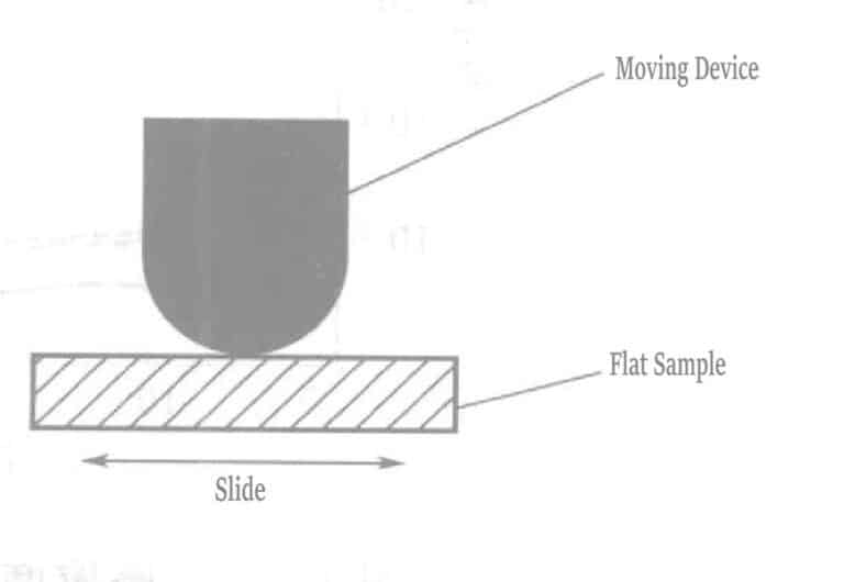
Table 1-151 Experimental Materials
| シリアル番号 | Slider | Flat plate |
|---|---|---|
|
1 2 3 4 5 6 7 8 9 10 11 12 13 14 15 |
Copper plated 5μm Gold-cobalt plated 3μm Palladium material Palladium material Zinc-40 lead Gold-cobalt plated 3μm Palladium plated 4μm Palladium plating 5μm Palladium-20 nickel alloy 5μm plated Gold-cobalt plated 3μm-206D contacts Palladium plated nickel alloy followed by brush plating Au-206D contact Palladium plated layer followed by brush gold plating Galvanized 12μm Zinc plated 12μm lubricated Galvanized 12μm lubricated① |
Copper Stripping Material Copper stripping material Palladium plated 6μm Silver stripping material Silver-lead solution Silver-lead solution Palladium plating 2μm Palladium plating 5μm Palladium-20 nickel alloy plating 5pm Palladium-nickel alloy post-brush gold plating-206A Palladium-nickel alloy back-brush gold plating-206A Palladium post-brush gold plating Galvanized 7µm Zinc plated 7um Lubricated Zinc plated 7μm Lubricated① |
|
① After applying the lubricant, heat treat the slider and flat plate under 250℃ for 500 hours before the wear test. Note: Experimental conditions: 105 cycles, 50 gf load, 20μm amplitude, 1.4 Hz. |
||
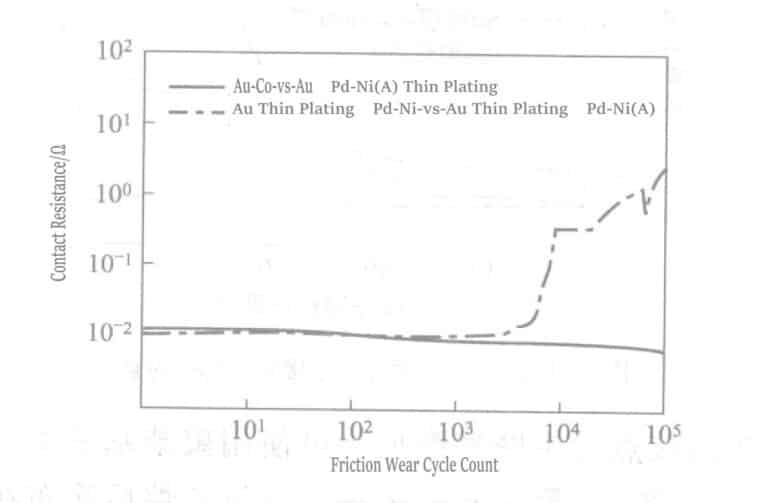
(2) Conclusion
① The performance of the palladium plating layer varies significantly depending on the type of plating solution. Figure 1-129 shows that the combination of palladium material and palladium plating layer (manufactured by Company A) demonstrates the performance over 105 cycles. The contact resistance value sharply increases after more than 2000 cycles. The wear of palladium initially involves adhesive wear movement, followed by spalling. Combining the same palladium plating layer (produced by Company B) shows slightly better performance. However, after 2000 cycles, the contact resistance value becomes unstable. The wear on the palladium-plated slider is less than on the palladium-material slider.
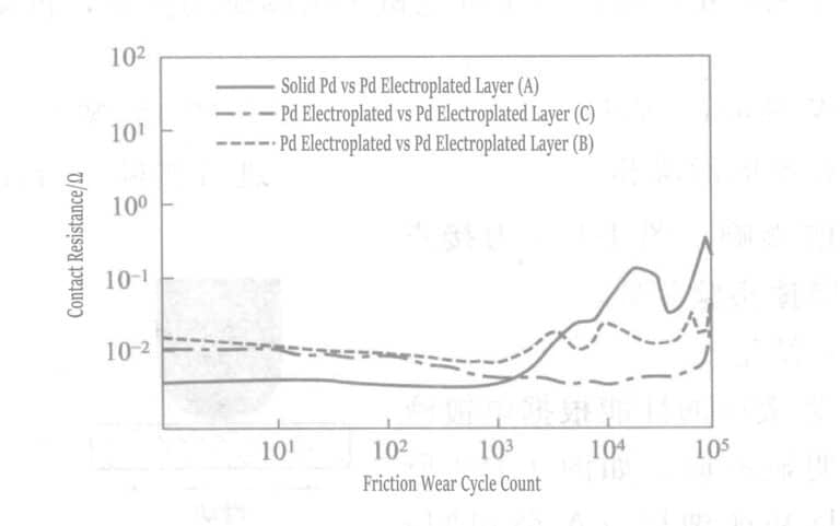

② Brush-plating gold can significantly improve the performance of palladium and palladium-plated layers. The palladium-nickel plating layer with brush-plated gold may experience friction, but this can be resolved by selecting an appropriate plating solution. The brush-plated gold palladium-nickel layers combined with hard gold can become an excellent plating series.
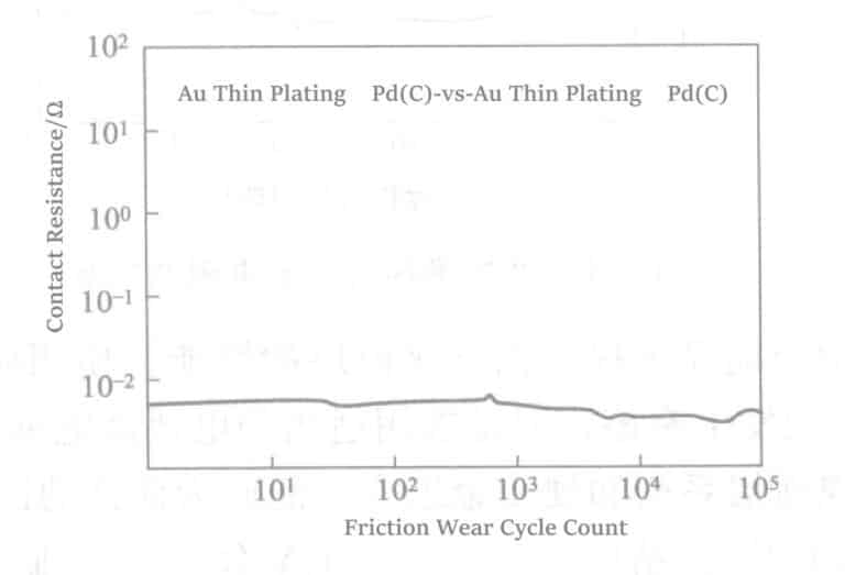
Figure 1-131 shows the wear conditions of the gold-cobalt plating layer combined with palladium-nickel (Company A) + brush-plated gold (0.1~ 0.2μm) and the palladium-nickel + the same brush-plated gold plating layer combination. The combination of the gold-cobalt plating layer and brush-plated gold palladium-nickel plating layer (Company A) did not increase the contact resistance value and did not experience friction wear. However, the same brush-plated gold palladium-nickel plating layer combination showed unstable contact resistance values after about 6000 cycles.
The friction of the tin coating can be addressed using lubricants, but the durability of the lubrication effect remains to be investigated.
As shown in Figure 1-133, the contact resistance value significantly increases after only a few hundred cycles for the same combination of tin plating layers, and a practical open circuit state has already formed within 3000 cycles.
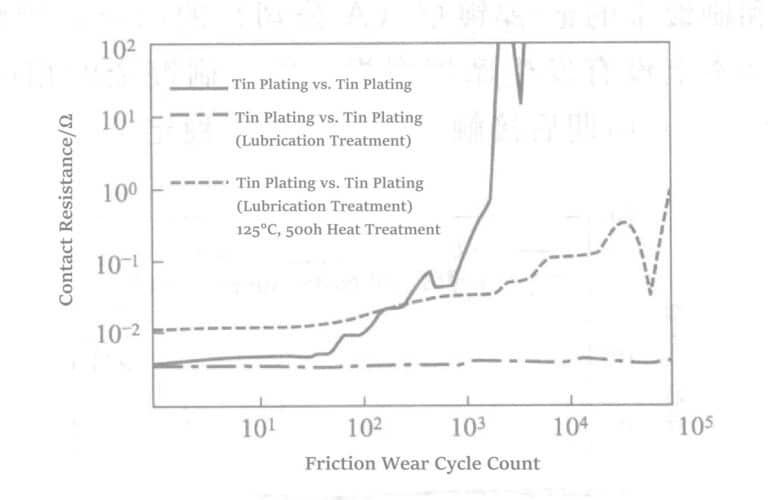
Polyphenylene ether lubricants (trade name ETinerp) can be used to prevent friction wear on tin-plated contacts. Dissolve 2% polyphenylene ether in trichloroethane and apply it to the slider and flat plate; use after the solvent evaporates.
No wear occurred after 100,000 cycles of friction on the lubricated tin-plated layer. To test the durability of the lubricant layer, the lubricated tin-plated slider and flat plate were heat treated under 125℃ for 500 hours, and then a friction test was conducted. The result showed that the contact resistance value was still much lower than that of the lubricated tin, indicating that the high performance before heat treatment could not be maintained.
Section II Methods of Gold Recovery
1. Overview
Table 1-153 Gold-Containing Waste and Waste Liquid from Electroplating
| シリアル番号 | Types of gold-containing waste and waste liquid | 特徴 | Recovery method |
|---|---|---|---|
| 1 | Gold deposited or attached to fixtures used for gold plating, and gold plating wastes | Mixed nuggets of gold, copper and nickel | Dissolve and neutralize with aqua regia, then use reducing agent to reduce and precipitate the gold, and take out the crude gold. |
| 2 | Gold attached to defective plated products. | Gold Stripping Solution | Replace the gold with aluminum and zinc powder in alkaline solution, and take out the crude gold. |
| 3 | Gold in the stripping solution after stripping the plated layer. | Stripping solution of gold | Same as 2 |
| 4 | Gold in grinding powder after grinding the plated layer. | Mixed chips with abrasive powder | After incineration, dissolve in aqua regia and recover by the method of 1. |
| 5 | Gold in plating line and cleaning water | Solution with low gold content and cleaning water |
Ion exchange method; Inorganic adsorbent adsorption method; Electrolytic recovery method
|
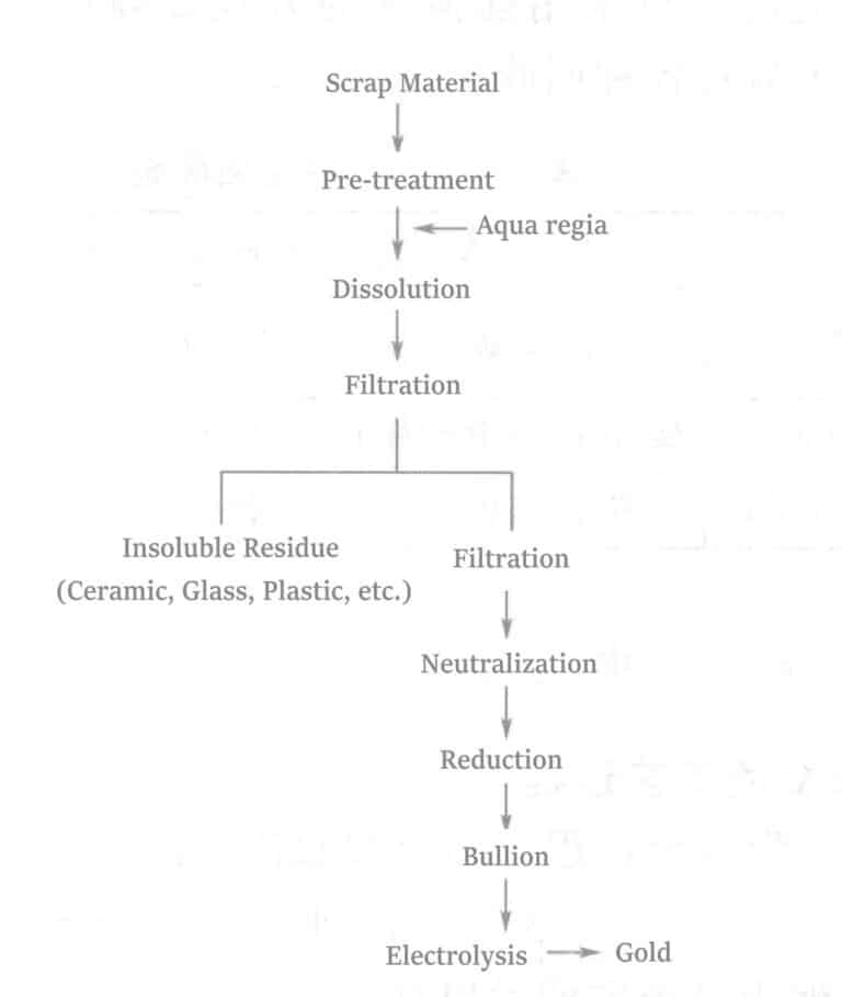
2Au + 2HNO3 + 6HCl → 4H2O + 2NO↑ + 2AuCl3
AuCl3 + HCl → HAuCl4
2HAuCl4 + 3SO2 + 6H2O → 3H2SO4 + 8HCl + 2Au
HAuCl4 + 3FeSO4 → 鉄2(SO4)3 + FeCl3 + HCl + Au
2HAuCl4 + 3H2C2O4 → 8HCl + 6CO2↑ + 2Au
Two types of gold-containing waste liquids are produced during the electroplating process. The gold concentration in the recovery tank is about several hundred 10-6 levels, while the gold concentration from the washing tank is very dilute, only 1×10⁻⁶ level.
The electrolytic method has the highest recovery rate among the gold recovery methods for waste liquid in the recovery tank. When gold is deposited at concentrations around levels, the gold concentration near the cathode is too low, so hydrogen gas is first evolved. At this time, strong stirring can increase the supply of gold ions to the cathode. Table 1-154 provides descriptions of various recovery tanks.
Table 1-154 Electrolytic Gold Recovery
| シリアル番号 | 方法 | Cathode shape | Gold Recovery State | Gold Recovery Methods |
|---|---|---|---|---|
| 1 | Fluidized bed type | Titanium and platinum plate | Plate, powder | Remove the cathode, dissolve the gold with chemicals or scrape the gold. |
| 2 | Rotary cylinder type | Titanium, platinum plate, stainless steel plate | Plate, Powder | Remove the cathode and scrape the gold |
| 3 | Metal microparticle type | Carbon particles, metal particles | Particles | Dissolve gold |
2. Recovery of Gold during the Gilding Process
2.1 The Process of Recycling Gold
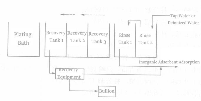
Figure 1-135 is the gold recovery flowchart during the gold plating process.
The gold concentration (200~300)×10-6 in pure gold plating solution has the highest recovery rate; when the gold concentration is high, a high concentration of conductive salt needs to be added.
2.2 Key Points for Configuring Recovery Equipment in the Plating Production Line
① The electrolytic tank and the production line with associated equipment should be as low-cost as possible.
② The structure of the assembly line and necessary functional parts, such as rectifiers, power supplies, and circulation spring systems, should be reasonably designed and configured.
③ The replacement and maintenance of parts should be easy to operate.
④ The operation of gold recovery should be simple (for example, the cathode can be easily removed from the electrolytic cell).
⑤ Waste liquid with very low gold concentration can also be effectively recovered.
⑥ Able to selectively recover gold.